Baru 37 Pcbway Tutorial Gambar Minimalis, Skema Pcb
Baru 37 Pcbway Tutorial Gambar Minimalis, Skema Pcb. Berikut Penjelasan lengkap tentang fungsi komponen-komponen skema pcb dari yang aktif hingga pasif, prinsip cara kerjanya serta simbol yang wajib difahami. Perhatikan komponen skema pcb jenis resistor berikut yang dilengkapi dengan gambar. Simak ulasan terkait skema pcb dengan artikel Baru 37 Pcbway Tutorial Gambar Minimalis, Skema Pcb berikut ini

Using PCBWay Free Gerber Viewer to Visualize Your PCB Designs Sumber : www.radiolocman.com

How to pick and place report by OrCAD PCB Layout Sumber : www.pcbway.com

How to pick and place report by OrCAD PCB Layout Sumber : www.pcbway.com

How to pick and place report by OrCAD PCB Layout Sumber : www.pcbway.com

How to Reflow Surface Mount SMD Soldering Tutorial Sumber : www.pcbway.com

PCBWay review YouTube Sumber : www.youtube.com

How to pick and place report by OrCAD PCB Layout Sumber : www.pcbway.com

PCBWay PCB prototype service review Electronics Lovers Sumber : www.electronicslovers.com

Complete series of PCB designing video tutorials Sumber : microcontrollerslab.com

pcbway ruller 2 Embedds Sumber : embedds.com

Making Your First Printed Circuit Board Getting Started Sumber : projects-raspberry.com

How to pick and place report by OrCAD PCB Layout Sumber : www.pcbway.com

How to pick and place report by OrCAD PCB Layout Sumber : www.pcbway.com

TUTORIAL on how to add a ground plane to a pcb in the Sumber : www.pcbway.com

PCB Prototype Service by PCBWay The Engineering Projects Sumber : www.theengineeringprojects.com
Using PCBWay Free Gerber Viewer to Visualize Your PCB Designs Sumber : www.radiolocman.com
PCBWay Temperature Indicator System Arduino Project Hub
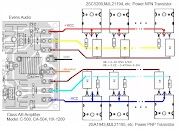
The PCB provides both the mechanical support for the components and is many cases is a critical part of the circuit since the length of tracks their thickness their clearance from other tracks and the relative placement of components and tracks can significantly influence the final performance of the PCB This is particularly true as power levels clock speeds or frequency increases
How to pick and place report by OrCAD PCB Layout Sumber : www.pcbway.com
pcbway com China PCB Prototype Fabrication Manufacturer
03 07 2020 by PCBWay Jul 03 2020 19607 Views 10 Comments Posted in Help Center Tutorial PCB design Kicad Gerber Usually it is easier to generate Gerber
How to pick and place report by OrCAD PCB Layout Sumber : www.pcbway.com
Reasons Why You Should Use PCBWay for Your Next PCB
As a full service PCB prototype and assembly provider PCBGOGO can cover all your pcb requirements including custom prototype and mass value fabrication high quality pcb assembly
How to pick and place report by OrCAD PCB Layout Sumber : www.pcbway.com
PCBWay unboxing capabilities and in depth board review
Therefore case you want your own PCB you can obtain through this link on PCBWay com website For this you can access the website create your account and obtain your own PCB s Comments Team members Sil cios Lab 32 Project tutorial by Michael Marinis and PCBWay
How to Reflow Surface Mount SMD Soldering Tutorial Sumber : www.pcbway.com
PCB prototype China PCB manufacturer PCB Assembly
PCBWay review YouTube Sumber : www.youtube.com
PCB prototype PCB Layout PCBWay
How to pick and place report by OrCAD PCB Layout Sumber : www.pcbway.com
How PCB is Made in China PCBWay Factory Tour YouTube
In this project you will learn how to build a system to function as a temperature indicator for Arduino By Sil cios Lab and PCBWay
PCBWay PCB prototype service review Electronics Lovers Sumber : www.electronicslovers.com
PCBWay Arduino Bicycle Odometer Arduino Project Hub
For Kicad 5 the documentation of pcbnew explains how to generate Gerber and drill files and can also be found in Pcbway s tutorial For other EDA software there are abundant tutorials on the Internet Package the generated files usually 9 as a zip archive and upload to the website At this point Pcbway will do a review of the files
Complete series of PCB designing video tutorials Sumber : microcontrollerslab.com
Generate Gerber file from Kicad Help Center PCBway
The rise of IoT Industry 4 0 and the smart revolution has triggered a butterfly effect on the electronics hardware industry This trend has led to electronics manufacturers having to innovate or be eaten by the competition It has also led to an influx of new bloods interested in taking over the electronics space and PCBWay is one of them Although everyone upsells their PCBs as the best in
pcbway ruller 2 Embedds Sumber : embedds.com
My experience using a PCB fab service Pcbway Ken Yap
Making Your First Printed Circuit Board Getting Started Sumber : projects-raspberry.com
How to pick and place report by OrCAD PCB Layout Sumber : www.pcbway.com
How to pick and place report by OrCAD PCB Layout Sumber : www.pcbway.com
TUTORIAL on how to add a ground plane to a pcb in the Sumber : www.pcbway.com
PCB Prototype Service by PCBWay The Engineering Projects Sumber : www.theengineeringprojects.com


0 Comments